Munich, 19 October 2026 · Nexuswelt Group
Most startups assume the Chips Joint Undertaking is about fabrication plants and therefore not for them. That assumption is wrong twice over: it misses the collaborative research calls, and – more importantly – it misses the fact that much of what the Chips JU funds is infrastructure you can use without winning anything at all.
This guide covers how the programme is structured, the design platform and competence centre network a startup can access directly, the national co-funding rule that catches applicants out, and where a small company realistically fits. For the broader starting point, see our guide to EU funding for startups.
Two pillars, funded from two programmes
The Chips Joint Undertaking manages two streams of investment, drawing on both Horizon Europe and Digital Europe.
| Pillar | What it funds |
| Chips for Europe Initiative | Strategic infrastructure that bridges research and industrial deployment: pilot lines, a cloud-based design platform, a network of competence centres, and dedicated quantum actions |
| Electronics Components and Systems Research and Innovation (ECS R&I) | Collaborative projects across a broad range of technology domains, through Research and Innovation Actions and Innovation Actions, with a Global strand opening topics to international cooperation |
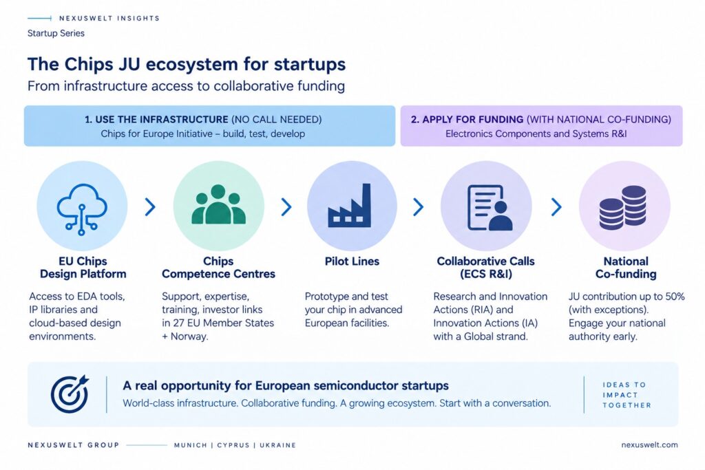
The distinction matters for a startup. The first pillar largely builds things you can use. The second is where you apply for project funding in a consortium.
The part most startups miss: infrastructure you can use
Three assets exist specifically to lower the barrier for small companies, and using them does not require winning a call.
The EU Chips Design Platform
A pan-European, cloud-based design infrastructure coordinated by imec and implemented by a consortium of European research and technology organisations. It gives SMEs, startups and fabless companies access to commercial electronic design automation tools, IP libraries, cloud-based design environments, and a route through to European pilot lines and manufacturing.
For a fabless startup, subsidised access to EDA tools and IP libraries removes one of the largest fixed costs in chip design. First companies are being onboarded across 2026 to 2028.
Chips Competence Centres
A structured network of thirty national centres established across all twenty-seven EU Member States plus Norway as of February 2026. They operate on an open and non-discriminatory basis and act as the first contact point for SMEs and startups.
What they provide: access to pilot lines and the European design platform, technical expertise and design support, skills development and training, help finding investors, and connections across the European network. Participating states define their own technological priorities, so the centre in your country is likely to be aligned with national industrial strengths.
This is the single most useful first step for a semiconductor startup in Europe, and it costs a conversation.
Pilot lines
Shared advanced-manufacturing facilities where companies can prototype chips they could not build alone – including lines for photonic integrated circuits and wide band gap technologies. Access is typically arranged through the competence centre network or through participation in a funded project.
The national co-funding rule
This is the structural feature that surprises applicants, and it does not work like Horizon Europe. For the standard Horizon Europe baseline, see our guide to funding rates and co-financing.
Most Chips JU calls are co-funded: the Joint Undertaking contributes a share and the participating state contributes the rest. The JU contribution is up to 50% for co-funded calls, with the coordination action for competence centres being an exception funded entirely through Digital Europe.
Two consequences follow, and both need attention before you invest in a proposal:
- Your national funding body’s rules apply alongside the JU’s. Eligibility, funding rates and reporting requirements are partly set nationally, and they differ between participating states.
- You must engage your national authority early. A proposal that succeeds at JU level but has no national funding commitment behind it does not proceed. This is not a formality to complete afterwards.
The practical instruction: contact your national funding body and your Chips Competence Centre before writing anything. In some participating states the national process has its own deadlines that precede the JU cut-off.
How the calls are structured
The ECS R&I stream runs annual collaborative calls spanning low to high technology readiness. Recent cycles have opened in early July with cut-offs clustered in September, covering areas such as power electronics, photonics, health electronics, quantum chip design, quantum enabling technologies, skills, and pilot line federation.
Two features worth knowing:
- Research and Innovation Actions fund lower-maturity work, including bottom-up calls at roughly TRL 3–4 aimed at establishing new knowledge and technical feasibility. Innovation Actions fund market-oriented development at roughly TRL 5–8, with a deployment plan for Europe.
- The Global strand, which opens topics to international cooperation, runs in two phases: a short project outline first, and a full proposal only if the outline succeeds. This is the same logic as a two-stage Horizon Europe call and it substantially lowers the cost of attempting.
Call dates and budgets change each cycle. Verify current opportunities on the Chips JU portal rather than relying on any secondary summary, including this one.
Where a startup actually fits
| Your position | The realistic route |
| Fabless design, need tool and IP access | The EU Chips Design Platform, and your national competence centre as the entry point |
| Early-stage concept, TRL 3–4 | Bottom-up Research and Innovation Action topics, as a partner in a consortium |
| Working technology, TRL 5–8, deployment ambition in Europe | Innovation Action topics, where industrial relevance rather than novelty is the scoring emphasis |
| Edge AI, accelerators, hardware-aware optimisation | ECS R&I topics – often a better match than a Horizon Europe Cluster 4 AI topic, with less competition |
| Need prototyping capacity you cannot afford | Pilot line access, arranged through the competence centre network |
| No consortium and no network in this field | Competence centre first, then the industry associations – this is where consortia form |
| Non-EU but associated country | Check the topic conditions and the national co-funding position, which is where the complication usually sits |
For a broader comparison of the available routes, see our guide to comparing AI funding programmes.
How consortia form in this ecosystem
This is the part that differs most from the rest of European funding, and it is why an outsider can find the Chips JU opaque.
Three industry associations partner in the Chips Joint Undertaking alongside the European Commission and the participating states: AENEAS, EPoSS and INSIDE. They represent research, development and innovation actors across the electronic components and systems value chain, from large industry and SMEs to research organisations and universities, and they contribute to defining strategic priorities and shaping the work programme.
Consortium formation runs heavily through these associations and their working groups rather than through open partner-search platforms. For a startup, that means membership and participation in the relevant association is not a networking nicety – it is the primary access route to the consortia that will submit. Compared with the cost of an unsuccessful proposal, it usually pays for itself.
Nexuswelt is a member of the INSIDE Industry Association, which is one reason this cluster is covered here in more depth than a general funding consultancy would.
Practical steps
- Contact your national Chips Competence Centre. It is the designated first contact point for startups, the conversation is free, and it will tell you what your national participating state supports.
- Establish your national co-funding position early, including any national deadlines that precede the JU cut-off.
- Investigate design platform access if you are fabless. Subsidised EDA and IP access changes the economics of early design work.
- Establish your TRL honestly, since it determines whether you belong in a Research and Innovation Action or an Innovation Action.
- Join or engage with the relevant industry association and its working groups, where consortia actually form.
- Register and obtain a Participant Identification Code, independently of any specific call.
- Use the Global strand’s outline phase to test an idea cheaply where international cooperation fits your case.
- Start as a partner. Coordination in this ecosystem is generally led by established industrial players and research organisations.
How Nexuswelt works with semiconductor companies
Nexuswelt is a member of the INSIDE Industry Association and works with deep-tech companies on programme selection, consortium positioning and the impact and exploitation logic these projects are judged on, contributing to funded projects as a partner for communication, dissemination, stakeholder engagement and exploitation. The wider policy context is in our guide to European technology sovereignty, and more on the firm is on the Nexuswelt about page. For companies still choosing between programmes, start with an EU funding options assessment.